In this post we continue our discussion of the charge carrier
concentrations. In the previouspost you have been introduced to the density of
states function, the Fermi-Diracdistribution and the fermi level. We will now
use these parameters to determine the chargecarrier concentrations in thermal
equilibrium.Let’s recap. First we discussed the band diagram, with its
well-defined bands for the valenceelectron energies, conduction electron
energies and band gap, where there are no energystates that an electron can
occupy.
Then we defined the density of states function. This function
is material dependent. Thedensity of states function therefore tells you the
number of states available for an electronto occupy at a certain energy level,
for a given material. In highpurity intrinsic semiconductor materials, there
are no energy states available for an electronto occupy in the bandgap.In the
next step we looked at the occupation of the energy states. For this, we
introducedthe Fermi-Dirac distribution function, also often called occupation
function.
This distributionfunction gives the probability that a
certain energy state is occupied at a certaintemperature. The Fermi-Dirac
distribution is a general rule, applicable to electrons in allkinds of
systems.Now, the last step is to determine the charge carrier densities in the
conduction and valencebands. This is what the profile of the occupied states
looks like.
On the top we can see theoccupation of the conduction-band states and
on the bottom we see the occupation of thevalence-band states. So how did we
get these profiles?The actual number of
electrons occupying a certain energy level, ‘n’, is equal to the product of
thenumber of available states, ‘g’, and the probability that a certain state is
occupied, ‘f’. As wediscussed, the probability of an electron occupying an
energy level above the fermi levelincreases with increasing temperature.
However, as there are no available states in thebandgap, no electrons will
occupy an energy level in the bandgap.If the temperature starts to increase
from the zero Kelvin, the probability of an electronoccupying an energy state
in the conduction band will become greater than zero.
This isalready the case at room temperature. The density-of-states
function is greater than zeroalso for energy levels in the conduction band.
Consequently, at room temperature someelectrons occupy energy levels in the
conduction band.If we want to know the total amount of mobile electrons, we
just have to integrate thisproduct from the conduction band edge through up the
band.A similar equation is used for the number of holes in the valence band.
However, rememberthat holes are simply the missing electrons at given states in
the valence band. Therefore,we have to multiply the density of allowed states
by one minus the occupation function, tofind out which states are
unoccupied.Again, we can integrate this product to obtain the total number of
holes in the valence band.If we use the Boltzmann approximations, we can calculate
these concentrations.
Forelectrons in the conduction band we get this expression
and for holes in the valence bandwe get this expression.There are two new
parameters in the equations for carrier concentrations, N_C and N_V.We call
these parameters effective densities of conduction and valence band
states,respectively. As you can notice they are different from each other,
since the effective massof electrons is different from the effective mass of
holes.Now we get to an important property of semiconductors: the intrinsic
carrier concentrationor n_i. n_i squared is equal to the product of n, the
concentration of electrons occupyingstates in the conduction band, and p the
concentration of holes occupying states in thevalence band.
This product can be calculated as follows. In the simplified
expression we can see that n_i isjust dependent on the bandgap, temperature and
effective densities of states. In a fullyintrinsic semiconductor, since n and p
are equal, they are both equal to n_i. For c-Si at 300Kn_i is equal to 10 to
the power of 10 cubic centimeters. We will use this value in manyequations to
come, so make sure to note it down.
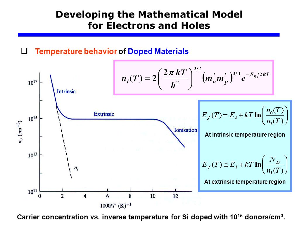
This graph shows the temperature dependence of charge carrier
concentrations in intrinsicsilicon. It can be expected that, with increasing
temperature, more electrons are excitedfrom the valence into the conduction
band since more thermal energy is available. Thisexplains the increasing
n_i.With this lecture you have learned how to determine the concentration of
charge carrierswithin a semiconductor.
However, this method is only valid for
intrinsic semiconductors inthermal equilibrium. In the following posts we will
first see how the concentration ofcarriers can be manipulated by doping the
material. Afterwards we will move our analysis toa non-equilibrium situation.
Comments
Post a Comment