We have discussed some important properties of light and
characteristics of the radiation of light by our sun. In this post, we will
focus on converting that light to electrical energy. This is done using the
photovoltaic effect. Photovoltaics covers the direct conversion of sunlight
into electrical energy, by a semiconductor material. The term photovoltaics is
derived from the Greek word ‘phos’ which means light, and volt, which refers to
electricity, specifically voltage.
Volt is a reference to the Italian physicist Alessandro
Volta, who invented the battery photovoltaic effect that was discovered in
1839, by the French physicist Emond Becquerel. At the age of 19 Becquerel
created the first photovoltaic cell by illuminating platinum electrodes, coated
with silver chloride in an acid solution.
This device was the first to convert light into electricity.
The photovoltaic effect occurs through the generation of a potential difference
at the junction of two different materials, in response to electromagnetic radiation.
The photovoltaic effect consists of three distinct processes. The first process
involves the absorption of light, which leads to the generation of charge-carriers.
During the second process, the generated charge-carriers are separated.
The third and final process consist of the collection of the
of the charge carriers at the electrodes.Let’s look at these processes in some
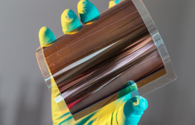
more detail. We will use the shown solar cell to visualize the photovoltaic effect.
This is a basic crystalline silicon solar cell, with an n-doped silicon layer,
a p-doped silicon layer and back and front electrodes. The first process
involves the absorption of photons in the materials that form a junction.
Upon absorption of the photons, an electron-hole pair is generated.
A negatively charged electron is excited to a higher energy state and it leaves
behind a positively charged hole. Here we show one photon of light exciting a
single electron hole-pair. In reality, there will be many electron hole pairs
generated at once with a full spectrum of light.This electron hole pair will
only survive for a certain lifetime. After some time, recombination may occur.
This means that the electron will fall back to its initial
energy state. If this happens, that absorbed energy is essentially lost and
cannot be converted into electrical energy. Therefore, in order to really
generate electricity we have to separate these charge carriers. How do we do this?
Once carriers are generated in a solar cell, they will move around due to
various processes such as diffusion, random motion and drift. In order to
separate the photo-generated charge carriers, semipermeable membranes must be
present on both sides of the absorber. This ensures that the electrons can only
flow out through one membrane and holes can only flow out through the other membrane.
In our solar cell here, the charges were generated in the p-type semiconductor.
As you will learn in later videos, the p-n junction at the
top of the solar cell only allows electrons to pass through and the junction at
the bottom of the cell only allows holes to pass through.Therefore, the solar
cell needs to be designed so that the mobile charge carriers eventually hit
those barriers and are separated. So now, we have GENERATED and SEPARATED
charge carriers, but we have one more step to generate electricity. The final
process then involves the collection of the photo-generated charge carriers.
Let’s start over again.
Under influence of light, a large number of charge carriers
are generated and separated. The difference in charge carrier concentrations at
both ends of the PV device causes a potential difference between the electrodes.
This potential can be measured by a voltmeter and is called the open circuit
voltage or V_OC. If an external circuit is applied between these electrodes;
electrons will flow from the N-type material towards the P-type material. There
is now a current flowing from a high potential to low potential, which is the definition
of electrical power.
This is how the charge carriers are extracted from the solar cells.
The chemical energy of the electrons-hole pairs is now converted to electric energy.
After the electrons have passed through the circuit, they recombine with holes
at a metal absorber interface. In summary, we have seen how the photovoltaic
effect involves the generation of charge carriers due to the absorption of
photons at a junction of two semiconductor materials, followed by the
subsequent separation of the photo-generated charge carriers. Finally, the
collection of the charge carriers happens at the terminals of the junction.
In an ideal semiconductor, electrons can populate energy
levels below the so-called valence band edge E-V, and above the so-called
conduction band edge, E-C. Between those two bands no allowed energy states
exist, that could be populated by electrons. The bandgap ‘E-G’, which is the
gap between the conduction band and valence band, is therefore also known as
the forbidden gap.
The bandgap energy is equal to the energy difference between
the conduction band edge and the valence band edge. Photons can only be
absorbed if the photon energy is equal to, or great than, the band gap energy. If
a photon with an energy smaller than the bandgap energy reaches an ideal semiconductor
it will not be absorbed, but traverses the material without interaction. The
absorption of a photon with sufficient energy leads to the excitation of a
valence electron to the conduction band. This excitation leaves behind a void
in the semiconductor lattice. This void behaves like a particle with a positive
elementary charge, and is called hole.
Comments
Post a Comment